|
 |
|
 |
|
 |
 |
|
G-1300, L.G.Floor, Chittaranjan Park,
New Delhi - 110 019. INDIA. |
Phone:
Fax:
Email: |
+91 11 2627 2117
+91 11 2627 2124
mail@geniustechindia.com |
|
 |
|
|
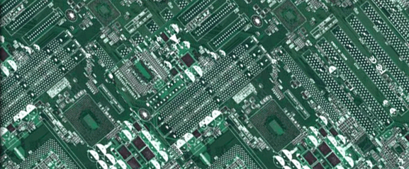
PCB Design Ball Grid Array indiaA Ball Grid Array or BGA package is a form of surface mount technology, or SMT package that is being used increasingly for integrated circuits. The BGA offers many advantages PCB Design Service India and as a result it is being used increasingly in the manufacture of electronic circuits. BGA has come into existence, to provide more robust and conventional PCB Design Service India package for integrated circuit with large number of pins in single board. The usual quad flat pack style packages had very thin close spaced pins, and these were very close control of the soldering PCB DesignService India processes or else the level of solder bridges and poor joints rose. From a design perspective, the pin density is moving PCB Design India away from the IC also proved to be difficult as there would be congestion in few areas. All the above problems solved by the BGA package, and improve reliability from the soldered joints.
What is a BGA package?
The Ball Grid Array is also known as BGA which uses some specific PCB Design Service India approach to the connections to which are utilized for more conventional surface mount connections. In the there is very limited space where lots of pins had to be mounted with very less space among the very closely and made much smaller to provide the required level of PCB Design Service India connectivity. The Ball Grid Array (BGA) PCB Design Service India uses the bottom of the package, where there is a huge area for the connections.
The pins are placed in a grid pattern on the surface of the chip carrier that is why it PCB Design Service India named as Ball Grid Array. Other way also you have to PCB Design Service India provided a connection that is pads with balls of solder are used as the method of connection. BGA device is fitted on the printed circuit board PCB Design Service India where there is a matching set of copper pads to make the needed connectivity.
It has not only improved the connectivity but lot of other advantages also. They provide a lower thermal resistance among the silicon chips itself than Quad flat pack devices. This PCB Design Service India permits heat generated by the integrated circuit inside the package to be conducted out of the device which makes the PCB Design Service India becomes fast and more efficiently. Through this it is quite possible for BGA PCB Design Service India devices to generate more heat without the need for special cooling measures.
In addition to this the fact that the conductors are on the underside of the chip carrier PCB Design Service India means that the leads within the chip are shorter. Accordingly unwanted lead inductance levels are lower, and in this way, Ball Grid Array devices are able to offer a higher level of PCB Design Service India performance than their QFP counterparts.
|
|
| home | about us | services | contact us | sitemap |
| |
Copyright © Genius Technologies Pvt. Ltd. |
| PCB Design Service India,
SMD PCB Design Delhi,
Multilayer PCB Design,
Printed Circuit Board Design Delhi,
Prototype PCB Fabrication, PCB Design India. |
|
|
 |