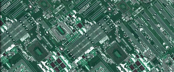
A printed circuit board is a component made of one or more layers of insulating materials with electric conductors. It is a thin board "printed" with electrical wires that are made from fiber glass. PCB Design Service India is mainly utilized in computer devices like motherboards, RAM chips, and network interface cards. In the multilayer the PCB Design India are fabricated with large numbers of wires over one to another with reliable set of predetermined PCB Design Service India interconnections for the electronic circuits.
There are lots of methods which can be performed these tasks. Few of these methods are handicapped through their reliance in a large number of chemical processes to condition the substrate. A lot of chemical PCB Design Service India processes are required to pass through tiny holes and electrolytic copper plate between the adjacent layers. Some common procedures is as follows:
- Gather all the material and equipment which you will require like as PCB Design Service India drills and electrolytic copper-plating cell.
- Separating the copper materials so that each can be easily and uniquely determined.
- With of help of special drilling machine use to make holes or vias.
- Correctly cleaning the copper substrates on your board.
- Electroplating the PCB Design Service India substrate using acid copper electroplating.
- Laminating the multilayer board.
High pressure PCB Design Service India and heat are required to fuse together. The conductors will be separated, and signals and power between layers will be connected. Here all the process be performed very carefully and each every steps should be ensured that all the layers are drilled properly and plated first, and then laminated. This can help reduce the number of chemical process required to perform this complex task. Multilayer PCBs which have 14 layers are quite too much expensive and so PCB with either 6 or 8 layers.
A multilayer PCB consists of two reference planes and a signal via. A signal via permits a PCB Design Service India signal to flow throughout the entire planes. A PCB Design Service India vias is connected to the planes just next to the signal via which serves to lessen the area so that the signal passes through. This is very PCB Design India significant as it helps to reduce noise and cross talk.
Multilayer boards might be rigid or flexible. Rigid multilayer PCB technology is too much PCB Design India expensive due more experience and the expensive drilling equipment is required. Flexible multilayer PCBs make use of flexible circuits which helps to decrease the size of the finished product. Benefits of PCB Design India multilayer PCBs are high reliability and uniform wiring. |