| |
|
G-1300, L.G.Floor, Chittaranjan Park,
New Delhi - 110 019. INDIA. |
Phone:
Fax:
Email: |
+91 11 2627 2117
+91 11 2627 2124
mail@geniustechindia.com |
 |
 |
|
|
|
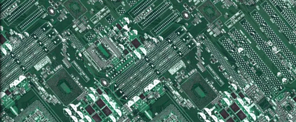
Some of the problem encountered in modern day printed circuit boards as circuit boards have become more inexpensive and reusable made:
- Capacitance in the board: To make printed circuit boards leak proof non-conducting material so that signals don’t from one lead to another. To make best insulator significant dielectric PCB Design Service India constant is used. This make the circuit as if two signals are routed over top of one another then sandwich of the signal and the dielectric will act like a capacitor.
- Inductance in the leads of a chip: earlier to the BGA PCB Design Service India there were Quad Flat Packs (QFPs) whose leads coming out of the sides. The leads which are coming out of the sides varies in thickness, but usually get thinner as there are more leads on a chip and the inductance of those leads goes up while the leads get thinner and longer. We remember PCB Design Service India that inductors are the “opposite” of PCB Design Service India capacitors in that they permit low frequency signals to pass and block high frequency signals. Inductors are the bad conductors and opposite of the capacitors in which they allow to pass very low frequency signals to pass and block high PCB Design Service India frequency signals.
- Timing: In a high speed system which needs signals to depart from a component at a certain time and arrive to other component some what later and there are lots of things which can PCB Design Service India prevent the signal from arriving undisturbed. Each and everything has some amount of resistance, the lines in a board routing one component to the next can have an affect on the overall performance of a PCB Design Service India circuit. If any of these lines is longer to the other than there will be an obvious difference of that line. While evaluating the impendence of two different lines going between components, differences can cause the signals to arrive at different times in unusual conditions.
- Ground/Power Plane: The most benefits which is brought by multilayer circuit boards is the capability to route a plane of power or grounding plane bottom a portions of a design. This technique is beneficial PCB Design Service India when you have a large connector that needs a majority of pins to be the same net. And with the grounding technology all of the pins on a circuit board that are tied to ground will technically be at PCB Design India ground, if it happens that one of the pin to be large current going into the ground into the ground, then that area would be slightly some higher potential in comparison to other areas of the grounding plane.
- Heat/Warping: The most PCB Design Service India disadvantages of the PCBs is the inflexibility of the material and when it heats up, it can often distort and become unusable. It would be a issues in acid etched and wire wrap boards, however since the connections are often either larger traces or wires, the chances which the warping would break the connection are often either PCB Design Service India larger traces or wires, and chances which the warping would break the connection are lower.
- Low Power: If one to built high power circuit PCB Design Service India need more care when high voltage or high currents is used. So the present new board also helps to save power savings, so high power situations are not as much of a main concern for the tools which make PCB Design Service India.
|
|
|