 |
|
G-1300, L.G.Floor, Chittaranjan Park,
New Delhi - 110 019. INDIA. |
Phone:
Fax:
Email: |
+91 11 2627 2117
+91 11 2627 2124
mail@geniustechindia.com |
|
 |
|
|
|
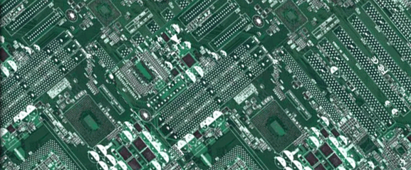
Nowadays Printed Circuit Boards PCB Design Service India is used to provide more efficient signals from one component in a circuit to the next. There is having multiple layer circuit boards with printed metal wires that connects with the entire component to make successful transfer of data. Before this there were different PCB Design Service India variation and precursors to the PCB Design Service India such as point to point wiring, wire wrap boards, acid etched copper on dielectric. All types of boards had lots of different methods but also had less restriction than today’s designs.
The difference lies in between the older boards and circuit design to today’s designed circuit are:
- Speed: It is fact that today denying the boards of today are faster in PCB Design Service India comparison to the old boards. The need and demand of the newest technology in the electronic media have let the industry to develop fastest and reliable circuit board to provide a real plat form for the navigation of data. Today’s the most demanding PCB Design India sector is cell phone. When the frequencies get into the GHz range and the signal is trying to guide signals instead of wire them, you know that your boards will be fast. As in the technology is growing at a very fast rate and number of PCB Design Service India user is also increase at tremendous rate, so speed is not limited to the RF industry because many latest designs have some PCB Design India component of a clocked digital system on integrated on them. It is also difficult to change it into the MHz range to the older board techniques. Making circuit point to point is not as PCB Design Service India workable with high speed signals, especially to the 32 wires between two components.
- Size/Type of components: As the demand of technology is of smallest and light in weight of the products like mobile. As the demand of mobile is growing and the demand of large PCB Design India sized products is now being prohibited. This trend has made the board a huge change ranging from each component to the surface Mount Technology. The smaller parts would also PCB Design Service India consume less power for running as compare to the larger sized components.
- Number of connections: The common type of today’s connection is known as BGA (Ball Grid Array). This kind of package uses little solders balls on the bottom of the package to adhere to the boards. It is stacked quickly after refold the balls fall into place on whatever PCB Design Service India you have produced. BGAs are ranging from 144 pins to 1000 pins per part. It is tough to wrap 1000 pins in board.
- ROHS: Lead is bad for the environment for your health and for any children who decide to ingest it. In fact, the only people who speak the wonders of lead these days are cranky analog engineers trying to solder PCB Design Service India something. Lead is more preferred as it has lower melting point and higher thermal capacity. That is the main reason RoHS is widely used with the silver-Tin solder.
|
|
|