 |
|
G-1300, L.G.Floor, Chittaranjan Park,
New Delhi - 110 019. INDIA. |
Phone:
Fax:
Email: |
+91 11 2627 2117
+91 11 2627 2124
mail@geniustechindia.com |
|
 |
|
|
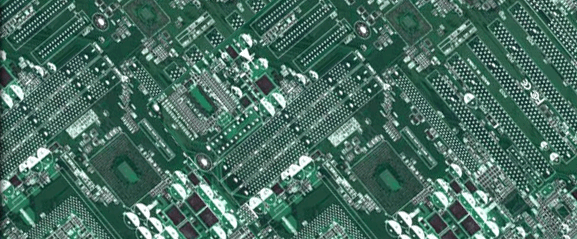
PCB Design Circuit Board for Assembly |
|
We are customer centric PCB Design Service India Company. We provide full services within time, in a rapid turn in the EMS environment. We offer high technology PCB Design Service India assembly solutions which would help to meet the whole of our customer’s electrical and mechanical requirements to have a better and effective solution.
Designing a Printed Circuit Board PCB Design Service India for Assembly is too difficult to GTs who outsources PCB Design Service India for design and manufacturing purposes. If properly accurately carried out performed, it shortens the time of product cycle, decreases the development cost, and gives a smooth flow into production from prototype phases. The production engineering team often hastens PCB Design Service India and development cycles. It fails to place emphasize on high volume production concern like fixtures etc. Every product of PCB Design Service India prototype engineers intended test the product immediately PCB Design Service India completion of all phases of design and to make sure that all the validation is performing rather than emphasizing PCB Design Service India for Assembly deliberation of the product.
The most appropriate approach for PCB Design Service India is to firstly observe the volume of production deliberations. The major cause is there are many different DFA deliberation associated to prototype PCB Design Service India assembly against production of PCB assembly. Each and every need some PCB Design Service India excellent expertise skill set for PCB Design Service India and equipment. If any of mistaken happens and right approach is not followed then the costs can rise and debugging the product can be pricey which will make heavy losses. In phase of prototype, validity of the connection of each route of flow and PCB Design Service India functionality of the circuit board is too significant than the testability and manufacturing rule which are very essential to apply at the PCB Design Service India production level to create the production smooth and flawless.
PCB Assembly Services
- Rapid turnaround for low to mid volume EMS
- High volume offshore PCB Design Service India
- Turnkey Assembly
- Shipment or partial shipment assembly:
- Design For Assembly: we provides DFA services to confirm layout, and programming for on time starts
|
|
|