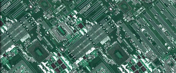
A PCB Design layout Delhi, or PCB, is used to mechanically support and electrically connect electronic components using conductive traces, etched from copper sheets laminated onto a non-conductive substrate. It is also known as Printed Wiring Board (PWB) or Etched Wiring Board layout. A PCB populated with electronic components is called PCB Design India (PCA), also known as a PCB Design layout India (PCBA).
PCBs are rugged, flexible, Rigid-Flex, one layer, two layer and multilayer. They require much more layout effort and higher initial cost, but are much cheaper for high-volume production. Most of the electronics industry's PCB design, assembly, and quality control requirements are set by standards that are published by the IPC organization.
One layer or Single Sided PCB consists of only one conductive PCB layout India typically made of thin copper foil on one side of dielectric.
Two layer or Double Sided PCB consists of two conductive layers typically made of thin copper foil on both side of dielectric.
Multilayer PCB Design layout India are called so as it has more than two layers like 4, 6 and so on. Conductive layers are insulated with dielectric made of epoxy resin called prepare.
SMD PCBs are called so as SMD (Surface Mount Devices) Components are populated on these PCBs using Surface Mount Technology. SMD Components are much smaller in size compared to conventional through-hole components, therefore smaller PCB is required which is need of Electronic Industries keeping compact size of equipments in mind. SMD PCB can be one layer, two layer or Multilayer.
PCB layout India
- Rapid turnaround for low to mid volume EMS
- High volume offshore PCB Design Service India
- Turnkey Assembly
- Shipment or partial shipment assembly:
- Design For Assembly: we provides DFA services to confirm layout, and programming for on time starts
|